PCB Layout & Design
Company Information:
Name: |
PCB Layout & Design |
Category: |
|
Offered by: |
|
PCB Layout & Design Description:
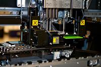
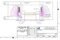
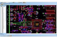
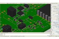
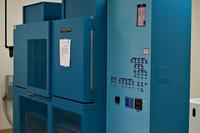
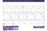
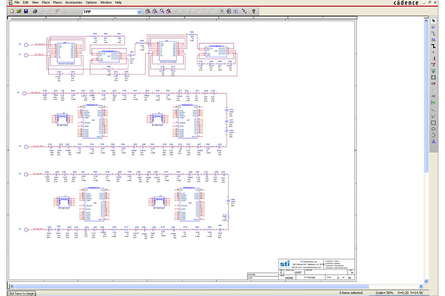
Even the best schematic circuit design can be undermined by poor component layout and routing. STI’s experienced design engineers address the critical design factors that affect manufacturing and assembly, product performance, and long-term reliability. The PCB layout and design services offered by STI combine experienced electrical, mechanical, thermal, manufacturing, and test engineers’ knowhow to ensure that the resulting PCBs fly through assembly, test, and ultimately to field thus helping to reduce product development costs.
- RF Design
- Tuned Routing
- Shielding
- High Speed Routing
- Bypass/Filter Component Placement
- Controlled Impedance Routing
- Matched Length Rules
- Differential Pair Routing
- Forward/Backward Annotation
- Library Creation and Maintenance
- Land Pattern Optimization
PCB Layout & Design was added in Apr 2016
PCB Layout & Design has been viewed 769 times
18 More Products from STI Electronics :