Feb 16, 2012
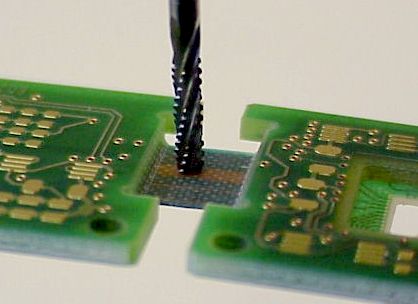
by Volker Feyerabend, APROS Int. Consulting & Services
The market's demands for finer structures have grown considerably over the years. Aside from smaller components, PCB dimensions for rigid and flex circuits have become increasingly smaller and lighter. Therefore, the products have been made smaller and faster. In effect, one technology has been a driver for the other. As miniaturization trends continue this course will make technological improvement and design creativity in the PCB production process indispensable.
Increases in component packaging density and the demand for more functionality have continued to drive design rules toward achieving a higher and higher interconnection density. With new designed circuit boards, one must deal with increased complexity and smaller tolerances. Therefore the need for accuracy has reached a new level and designers and manufacturers are faced with smaller tracks and vias.
In the context of drilling and routing, laser technology has enjoyed a fair share of publicity. For a long time, some considered laser technology to be the replacement for traditional mechanical processing. Lasers might play a leading role in current and future market demands, but there still are a lot of questions to be answered and a long way to go in terms of productivity and flexible capabilities.
The new market specifications for precision and tolerance can be supported by mechanical processes. Therefore interest in mechanical drilling and routing processes is still on the radar. During the last years, improvements in drilling machine capabilities have been achieved. Drilling productivity is no longer an issue today with the current generation of drilling machines and new technologies in place like dual spindle technology, (see my article on Dual Spindle Technology). Linear motors allow substantially improved path accuracy in routing and routing of complex forms. Precise definition of micro-vias, hole geometry, excellent hole-wall condition and accurate depth control allow for further options beside ‘standard’ drilling.
Mechanical circuit board processes however have some advantages like easy adjustments or lower costs. Over the years mechanical drilling and routing had been developed quite significantly. There is a new generation of demand in the market for system capabilities, tolerances and applications. The market shows a trend to flex and flex-rigid boards. Certain microwave designs where relatively large surface areas have to be crossed is a special challenge for routing and controlled-depth milling. All of this displays a clear trend towards multiplicity and flexibility which needs to be offered by equipment manufacturers.
The Swiss Posalux machine analyzed below, allows depth routing with an accuracy of +/- 15.0 um. Up to now, this seemed impossible with the focus being only on laser technology. However the strength of a drilling machine is still accuracy based performance. The depth routing option allows for very complex designs, bended boards and structures to be processed with fine precision.
A customer evaluation project for the advanced depth routing use of a routing system had been performed. I will share some valuable results and capabilities with you.
Depth routing technology- applications
To offer a structure, I will differentiate three areas of applications for the use of depth routing.
Option 1 is routing the top of the surface
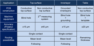
Pocket routing for components is used on rigid-flexible Printed Circuit Boards. The top surface will be milled away (taking the height of the chip and board into account). Considering a larger area must be traversed, the detection of the real surface structure is a key element. With non conductive top surfaces a 2nd measuring system is needed. Different detection and calculation methods, (see below), can be used. An accuracy of +-40 um is achievable with non conductive surfaces and +- 15 um on conductive spots. Pocket routing is mainly used if you need smaller boards and a lower board thickness for buried processors or resistors.
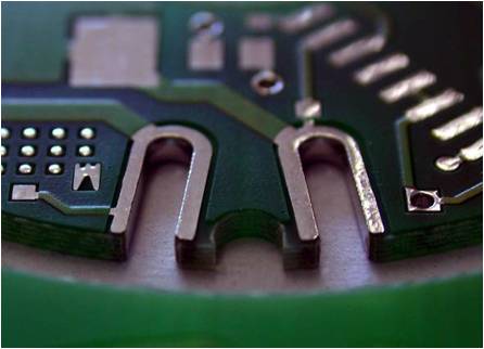
Option 2 is routing down to the innerlayers
In some applications a board needs to be designed with grounded innerlayers and free contact surfaces on an innerlayer, which are required to be connected to a chip. Designs should avoid tracks around the hole and above the chip. A nearby contact could falsely report the system as a closed loop and cause a false measurement, guiding the spindle to an undesired position. Customers currently use up to 12 layers in standard practice and production. The main reason for OEMs to use this kind of design is space, speed (shorter tracks) and EMC requirements. Technology-wise there are no limitations in layer count. As more layers are added, it becomes more difficult for the system to detect the right target layer and to measure the depth.
This type of depth routing technology allows designers to sink in a chip below the board surface and design a second chip above it. Routing leaves a square donut in between the connections of the two chips. Accuracy is within +/-15 um.
This advanced design causes less EMC problems due to the symmetry and the short distance between the components instead of using long tracks to connect them. But the real challenge is to evacuate the heat from in between the two components. This issue can be addressed by implementing an air channel and the integration of heat pipes.
Option 3 is routing semi flexible FR4 and rigid-flexible PCBs
Depth routing for semi flexible FR4 and rigid-flexible boards will be used if your board designer requests a bended board (which can be folded once). A part of the board will be milled away with an accuracy of +-20 um. As a result, the board can be bended, less space is needed and the product therefore can be smaller in size. Because there is no conductive area in which to measure, the table of the drilling/ routing machine will be used to detect the depth (detection methods see below).
Detection methods to control depth
In all of these applications the special challenge has to do with depth controlled drilling and milling. CO2 laser systems naturally stop cutting when contact has been made with the copper on the innerlayer. Mechanical systems require very precise measurements and feedback to achieve exact depth control. With the different available applications and products available, various measurement types are possible and necessary.
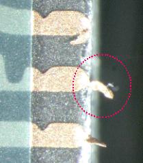
‘Contact drill’ and routing with single contact measurement
With 'contact drill' each hole is individually measured. Through this method, the desired result (through mechanical micro-via drilling) can be achieved. The drilling tool is electrically connected and makes contact with the copper foil surface. A known zero reference determines the hole depth. Base material warp is compensated and the consistent hole depths are ensured.
This becomes more difficult when we talk about routing. With a single contact measurement, surface determination will be done at the tool entry location. The only reference point is the entry point and therefore the depth remains constant during the entire routing process. The milled depth depends directly on the uniformity of material thickness. For relatively small boards and well defined top surfaces, traditional ‘one point/ single contact’ depth measurements may suffice. Though, it is seldom that single contact routing is used in the industry.
With thinner laminate layers and when areas get larger, it becomes more important to take the real differences of the substrate surface and thickness into account. Continuous monitoring and measurement or mean calculation become necessary.
‘Contact drill’ and routing with mean level measurement
With mean level measurement the surface level is measured at several locations. Several points with an electrical loop will be used. With the measured points and the received data, a mean contact level is calculated by interpolation. The routed depth is kept constant by the 2nd measuring system (also called floating). The system allows for a depth-control accuracy of +/- 15 microns throughout the operation.
Routing with second measuring systems
Surface detection with a second measuring system does not need a conductive surface. Routing is accurately controlled by a Z axis servo. There are two measuring systems per spindle. The first determines the exact height of the tool at the point of entry. The reading head is fixed on the drilling head. The second measuring system is linked to the Z axis controller and controls the Z-axis cutting depth and continuously compensates for surface topography. The linear scale is mounted on the pressure foot.
As soon as the pressure pad touches, the reading head starts to count. At first the difference between the tool and the pressure foot is measured. Then the routing process begins (with the calculated depth). This measurement method is less accurate (+- 40 um) than using a contact loop. Therefore a workaround for BGAs is sometimes used. A single sided copper foil on the backside of the chip can be integrated and a measurement can be done from there.
The pressure foot is also necessary because of the real board topography. The pressure foot will be used to achieve better results for applications with the flatness deviation of > 0,4-0,5 mm. The foot eliminates board lifting by providing downward pressure. This allows you to mill, rout and drill without boards lifting from the table during the entire process.
Additionally, a single-spindle machine can feature optical registration and monitoring with a CCD camera. The routing picture will be aligned to the printed image. The camera recognizes the fiducials and will correct measurement calculations and apply them to the routing system.
Second measuring system routing with “following method”
The most advanced method to measure depth is the “following method“. The spindle runs 2 times. First it runs to find the conductive surfaces and then to rout. The copper’s thickness needs to be at least 15 um minimum. The major disadvantage of the “following method” is speed. The method is approximately 200-250% slower than the mean method.
Bottom of panel referenced routing
With non conductive top surfaces, the bottom of a PCB will be used as a reference to calculate the depth. This routing type is mainly used for rigid-flex FR4 boards. The automotive industry with applications like dashboards or ABS systems and the telecommunication industry with mobile phones drive this technology in the main. The contact drill method is used to map an aluminium template. This mapped template data is used during the routing to correct the routing depth. This type of method is also used to separate the rigid-flexboard.
Herbert Kläy, Director of the PCB division of the Swiss Equipment manufacturer Posalux, shared his views about the process and the future of the technology. “Today’s customer’s needs, for productivity and accuracy, (with the miniaturization and the new set of products) can be handled with the above mentioned methods and technologies. Even aluminium backed up PCBs for LEDs and the automotive industry can be processed. In our developmental strategy it is expected that more R+D developments and improvements will be made over the next coming years.”
The development of CO2 lasers should also be watched closely, but as of today, lasers are no real alternative for depth routing. If one has to deal with large areas and larger material volumes on boards, productivity is the main challenge and R+D departments have only started to experiment with the technology for depth routing. When it comes to larger boards heating up, limited flexibility and scanning processes become additional problems. Therefore the laser technology has not been fully spread out in the market yet, although short-term laser depth routing may be an alternative for small boards or build-up technologies on substrates. In a couple of year’s time it will be apparent if the laser technology path will be cost-effective. Laser machines can be up to 1-2 time or more than the price than single drilling machines. The productivity benefit may also be visible if you have many blind holes on your products. Due to budget reasons, most laser drill systems using a single laser source limit speed and productivity. Many laser systems are using > 4 J/cm2 for opening the Cu surface. With organic materials like polyimide or exposy resins, only 100 mJ/ cm2 is needed. This is a wide spectrum and the laser system demands a very advanced energy control to handle the various types of drilling steps.
The System’s flexibility is also limited due to the fact that you must first decide which wavelength is best, considering you have the ablation performance, materials and absorption ratio in mind. The laser spot size (which is 70 um with CO2 lasers) is an additional challenge in drilling microvias. Another constraint is the mechanical board design which might not deliver the same quality and repeatability in the micrometer range. Therefore there is still sufficient scope for the use of mechanical drilling and routing.
The Swiss drilling and routing machine can be configured with asynchronous drilling and routing spindles, which have a rotation speed range from 15‘000 – 125’000 rpm and a tool diameter range of 0.1 – 6.35 mm. If larger diameters and standard PCBs are used, synchronous routing spindles with a high torque at low speed and a speed range of 5‘000 – 60‘000 rpm can be used. In this case maintenance is lower and spare parts are relatively easy to find.
In Conclusion
Mechanical routing technology is ideal for PCB manufacturers who target high tech markets and prepare themselves for the customer’s demands of today and tomorrow. Depth routing technology supports a high end market with the need for accuracy, miniaturization, process stability and the need for productivity.
Key markets for routing technology include: telecommunications, automotive as well as niche markets such as aerospace.
A significant advantage of the mechanical routing process is flexibility. Mechanical routing processes can offer a wide range of applications and the use of organic and non-organic materials like polyimide or exposy resins, copper – brass PCB with ceramic insulation layer and alloy (aerospace products). Routing with oil mist for non-ferrous materials is also available.
Automatic tool changes and spindle direction turns (reversed rotation) offer accuracy and productivity. Due to this fact, burr issues will be reduced by routing from both sides. The different applications and detection methods to control depth offer a wide range of products which can be utilised.
The Swiss Equipment manufacturer developed a sophisticated interpolation algorithm which improves the accuracy and productivity while routing complex contours. This method also considerably reduces the tool wear and increases the lifetime of the routing tool.
To use the described design options, some depth routing manufacturing know-how and the right equipment is necessary. Therefore a close relationship between designers and PCB manufacturers has proven to be helpful.
Moreover, in various markets there is a rising demand for this kind of high-end technology. And as of today, some PCB shops and markets might stand a better chance to differentiate themselves from their competitors.
---- Foot notes ----
The Swiss manufacturer is Posalux. Posalux is a leading Swiss equipment manufacturer. The company builds high-tech drilling and routing machines for the PCB industry and special EDM and laser drilling machines for the machining of holes into nozzles for direct fuel or diesel injection for the automotive industry.
Volker Feyerabend is President of APROS Int. Consulting and Services (www.APROS-Consulting.com). He has a degree in Engineering and Economics. He has worked for Hewlett Packard, Agilent Technologies, Groz-Beckert in various international senior management positions. He also headed a European Outsourcing Organization with the focus on EMS/ PCB companies. Contact him at Info@APROS-Consulting.com.