Sep 14, 2021
 In the world of makers, people enjoy the fun of designing and developing hardware/ software, even final electronic products. They will not concentrate a lot on the cost and manufacturability. But it is quite different from lab to factory, when it comes to the PCBA manufacturing process, things become more complex. Many things should take into account, such as the cost, time to the market, and manufacturability.
This time, I will talk about 10 most often made mistakes when makers/ startups/ engineers developing PCBA for new electronics hardware products. Such as technical errors in the electronics design, PCB circuit design, manufacturability of PCBA enclosure, and some more general PCBA development mistakes often made by first-time developers.
1. Bad Consciousness on DFM - Design for Manufacturing
People often underestimate the complexity of developing a new PCBA and new physical hardware product and underestimate the complexity of manufacturing it. For many products, it takes almost as much time to manufacture as it takes to develop it, and sometimes even more. The cost of a PCBA manufacturing setup may also be as much or more than all your development costs.
In the entire PCBA design process, it is crucial to consider manufacturability as the primary. This process is called design for manufacturing (DFM). Nothing can slow down your time to market more than designing a product that cannot be effectively manufactured. In a word, implement the DFM practices as early as possible, to simplify the manufacturing, both in PCBA and enclosure.
The old way of thinking is that engineers develop a product (including PCB, PCBA, enclosure), then pass it to the manufacturer or the manufacturing department of a big company, then they're going to find out the way to actually manufacture it. There's almost no interaction between engineering and manufacturing. This is often a terrible way of development, all of us should abandon this process. It's far better to think about manufacturing from the beginning of PCBA development. For example, an easy design change in PCBA can have an enormous impact on making a product easier and faster to manufacture. For many electronic products, the 2 main manufacturability requirements are that the PCBA is designed for testability and the housing is designed for injection molding.
2. No Design Review
If you don’t get an independent design review of your product before you PCBA prototype and product prototype, then you'll be throwing money away. No matter how good an engineer is, nobody is ideal, and everyone makes mistakes. Getting custom PCBA prototypes and product prototype made is not cheap, whether it’s the electronics or the product’s enclosure. The more prototype iterations you need, the more it'll cost in total. It'll also take a longer time to develop and slow down your schedule of bringing the product to market.
One of the simplest ways to decrease the prototype iterations required is to ask for a second opinion, which is called a design review. Successful tech companies always require their engineers to carry design reviews to get feedback from as many other engineers as possible. Unfortunately, many makers, startups, and small companies make the mistake of completely skipping this critical step. That’s fine if you've got the talents to sufficiently review your design yourself. But if you don’t, do get a design review from others, especially for PCB, PCBA, and enclosure design!
3. Waste too much time on Estimate Manufacturing Cost
This is an important one. Good tech companies always know approximately how much a product will cost to manufacture well before they start full development. It is the PCB cost, PCB assembly cost, testing cost, enclosure cost, product assembly cost, certification cost, etc. Otherwise, how can they know whether the product is worth developing or not?
If you’re not a billion-dollar tech company, you may first get your product fully designed. Once you've got the final PCBA prototype/ enclosure prototype/ product prototype, and you're able to start manufacturing, then you can finally estimate the whole manufacturing cost. What if you find that your PCBA/ product goes to costs more to manufacture than you expected? Of course, you can increase your sales price target, but that obviously is not a good idea, it is also not friendly to your customers...
You could also make some redesigns to lower the PCBA and product manufacturing cost. But it is also time-cost, especially for this worldwide IC shortage period, the components price changes every day, the long time you waste in the redesign process, the higher risk of long lead time and high cost.
So, why not made the right design in the primary time? For some reason, many people think that you can only accurately calculate the manufacturing cost after you fully develop the PCBA/ product. That's absolutely untrue in today’s world. With the proper experience, it's possible to accurately estimate the manufacturing cost for almost any product. This can happen well before any PCB layout or 3D modeling occurs.
You can ask support by a professional turnkey PCBA manufacturer to help on that, for example, Makerfabs have rich experience in turnkey electronics manufacturing solution, if you need to get an estimation of your product manufacturing cost, send us your production files, including the PCBA related(Gerber/BOM), enclosure related, etc. We will estimate the cost for you in 1-2 working days. We will also make free DFM checks to avoid the possible risk in the manufacturing process. Here are also tips about How To Check The PCBA Quotation from a supplier.
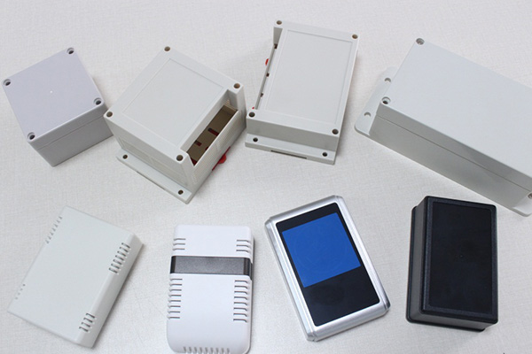
4. Not Manufacturable Product Enclosure
Think about a scene: you’ve spent all of the time and money getting the planning of your PCBA’s enclosure to look just right. It’s sort of an artwork to you, and this required a bunch of 3D-printed case prototype iterations to perfect its look and functionality. You finally have the right enclosure prototype! Now you need to find a manufacturer to produce them in mass, and you're ready to go. Right? What if I told you that your enclosure design is useless and you need to essentially re-design the whole thing? That might sound horrible, but this is a very common occurrence.

3D printing is powerful. You can design and print almost anything in your mind. But 3D printing is only for producing some prototypes. High-pressure injection molding is that the technology used for producing plastic parts in high volume. Unfortunately, injection molding isn't forgiving at all. it's a technology with many design rules that have been strictly followed. These rules are often so major, so limiting, on require a serious redesign just to make an enclosure manufacturable. It is very important to consider injection molding from the very beginning when designing your electronic product’s enclosure.
Also, as Makerfabs experience in enclosure, if all the things are ready and you don’t want to re-design your enclosure for some reasons, you can also Source a Proper PCB Enclosure for Your Project in the market, and ask Makerfabs to do some modifications to make it suitable for your PCBA, such as PCBA re-design, hole drilling, etc.
5. Not Manufacturable or Too Expensive PCB Design
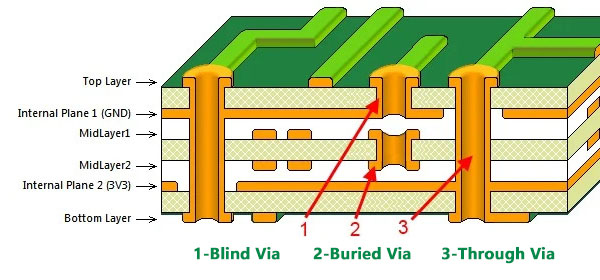
A via is a conducting hole during a PCB that connects signals from different layers. The most commonly known type of via is through via, because it goes through all layers of the board. That is, even if you simply want to attach a trace from layer one to layer two, all of the other layers also will have this through via. This may extend the dimensions of a PCB board since the vias reduce the routing space on layers not even using the via. A blind via, on the other hand, connects an external layer to an internal layer, and a buried via connects two internal layers. However, blind vias and buried vias have very strict limitations on which layers they can be used to connect.
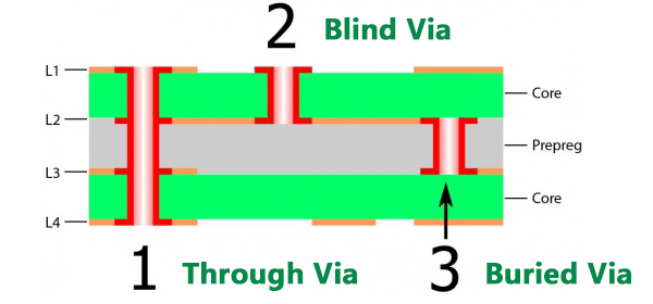
#1 is a through-via connecting all layers, #2 is a blind via connecting layers 1 and 2, and #3 is a buried via connecting layers 2 and 3.
In fact, the PCB is easy to be can’t manufacture and can’t prototype if using blind vias/buried vias. To know the restrictions of buried vias and blind vias, you should understand how the layers are stacked to make the PCB board. Be warned that, even if you use them correctly, blind vias /buried vias drastically increase the cost of PCB prototype boards. For most times, their use will double your PCB board cost, although this rise are going to be smaller once you reach higher production volumes. It's best to avoid buried and blind vias for most cases, unless you must have the PCB design as small as possible.
6. Insufficient Width for High-Current PCB Traces
If a PCB trace will have more than roughly 500 mA flowing through it, The minimum width allowed for a trace probably won’t be sufficient. The required width of the PCB trace depends on several things, including the thickness of the PCB trace (copper weight), and whether the PCB trace is on an internal or external layer. For the same thickness, an external layer can carry more current for the same width than an internal trace, because external PCB traces have better air flow allowing better heat dissipation.
Any PCB traces carrying more than 500 mA will need to be made wider than the minimum trace width.
The thickness depends on how much copper is getting used for that conducting layer. Most PCB manufacturers allow you to choose from various copper weights from 0.5 oz/sq. ft to about 2.5 oz/sq. ft. If preferred, you can convert the copper weight to a thickness measurement like mils. When calculating the current-carrying capability of a PCB trace, you must specify the permissible temperature rise for that trace. Generally, a 10℃ rise is a safe choice, but if you would like to squeeze down the trace width more, you can use a 20℃ or higher allowed temperature rise. Although the calculations for PCB trace width are pretty simple, I usually recommend using a trace width calculator.
7. Incorrect PCB Landing Patterns
All PCB design software tools include libraries of commonly used electronic components. These libraries include both the schematic symbol and the PCB landing pattern. All is sweet as long as you persist with using the components in these libraries. Problems begin once you use components, not in the included libraries. That is, the engineer has got to manually draw the schematic symbol and PCB landing pattern.
It’s very easy to make mistakes when drawing a landing pattern manually. For example, if you get the pin-pin spacing off by a fraction of a millimeter, it'll make it impossible to solder the part on the PCB board. A handy trick to avoid this error is to print out your PCB layout at a 1:1 scale. Then order samples of all of the varied components (mainly the microchips and connectors), and manually place them on your printed PCB layout. This enables you to quickly verify that each one of the landing patterns is correct.
8. Incorrect PCB Layout of Switching Regulators
A switching regulator converts one supply voltage to another by temporarily storing energy then releasing it to the output in a controlled fashion. The storage elements used are inductors and capacitors. Compared to simpler linear regulators, switching regulators are extremely efficient and waste very little power. However, they're far more complicated to use correctly. The biggest complexity of using switching regulators is correctly designing their PCB layout. You can’t randomly lay down the components and connect them up. There are strict layout rules you ought to follow for switching regulators. Fortunately, nearly all datasheets for switching regulators include a section discussing the right layout, also give an example of how to do it correctly.
9. Incorrect Use of Decoupling Capacitors
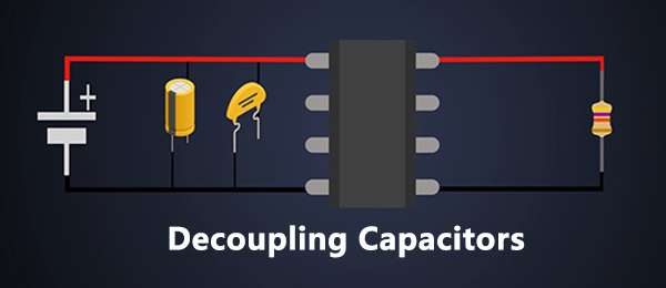
Critical components need a clean, stable voltage source. Decoupling capacitors are placed on the power supply rail to help in this regard. However, for decoupling capacitors to work their best they need to be as close as possible to the pin requiring the stable voltage. The power line coming from the power source must be routed so it goes to the decoupling capacitor before getting to the pin needing a stable voltage.
Also, it’s critical to put the output capacitor for the power supply regulator as close as possible to the output pin of the regulator. This is often necessary for optimizing stability (all regulators use a feedback loop that can oscillate if not properly stabilized). It also improves transient response. So it is important to use decoupling capacitors correctly.
10. Incorrect Wireless Circuit Design
If the PCBA has a wireless function, the PCB layout of any RF (radio frequency) part is very critical. Unfortunately, it does it wrong most of the time in wireless PCBA circuit design, so please pay close attention to it. For example, to achieve maximum power transmission between the transceiver (transmitter/ receiver) and the antenna, their impedance must be matched. This means that two things must be done.
The first is a suitable transmission line connecting the antenna and the transceiver. The transmission line is made on a printed circuit board and is specially used for the transmission of microwaves (high-frequency radio waves). There are two common types of transmission lines used in PCB circuit design: microstrip lines and coplanar waveguides. Microstrips are conductive strips separated from the ground plane underneath by a dielectric layer. A coplanar waveguide is similar to a microstrip line except that it adds another ground plane next to the conductive tape on the same layer. Of the two styles, coplanar waveguides are the most commonly used in wireless circuit design.
In most cases, the transmission line must be designed to have an impedance of 50 ohms to achieve maximum power transmission through the antenna. Do not confuse this impedance specification with the simple resistance of the line. The 50-ohm impedance refers to the complex impedance from the transmission line to the surrounding ground plane. I suggest you use a free tool called AppCad which is provided by Broadcom, to calculate the correct transmission line size.
In addition to using 50-ohm transmission lines, it is usually necessary to add some types of LC matching circuits, such as a pi network. This allows the impedance of the antenna to be fine-tuned for best matching and maximum power transfer.
Correct layout of RF transmission lines is essential. Using pre-certified modules is a good option.
One of the best ways to avoid these complications and lower the cost of obtaining product certification is to use pre-certified modules to implement any wireless feature.
For most wireless functions, there are two general design strategies: custom builds your own PCBA circuits with the appropriate microchips or use pre-certified modules with proven functions. Designing your own RF PCBA circuit is very complicated. In fact, it may be the most complex type of circuit to design correctly. Honestly, it's very likely that it won't be done correctly. It is to be expected that it will take many PCBA prototype iterations to get the correct operation. Another downside to a custom design is that it will add at least $ 10,000 to the cost of FCC certification. Using modules can reduce your profit margins, but maximizing your margin should never be your top priority.
Makerfabs can provide professional EMC optimization services for your wireless projects, to avoid the possible risks to your product.
For the product certification such as CE, Rohs, FCC, it is also important, which can make those electronics products ready to the market and sold legally to the end-customers. So if you need to make your product certificated, you can contact Makerfabs with your production files for a quotation. You can also check this article to know more about our PCBA/ Product Certification Service.
Conclusion
Those are the 10 most often made mistakes in PCB and PCBA development. The list is easy to expand, Makerfabs will meet different unexpected mistakes every day in PCBA manufacturing, and there is an almost endless number of mistakes waiting to be made! It is best to always know about potential pitfalls well before you actually get to them. That way, you can either avoid them entirely or at least be better prepared when they do occur.
Hope this article helps you to eliminate some of these potential errors in PCB design, circuit design, and enclosure design. However, the best way to avoid this type of mistake is to work with experts. It's always best if you hire the necessary experts right from the start to help guide you further, so you can avoid many of these kinds of mistakes before you go too far into the rabbit hole. You must at least ask independent experts to check the design before spending significant money on prototypes and manufacturing.
BTW, Makerfabs have rich experience in turnkey electronics manufacturing including the PCB, PCB assembly, enclosure, certification, product assembly, etc, everything you may need before your PCBA or electronics hardware product comes into the market. So do contact Makerfabs for some check, review, and quotation before PCBA prototyping, PCBA manufacturing, and product manufacturing. You're welcome to contact Makerfabs at service@makerfabs.com.