Nov 08, 2013
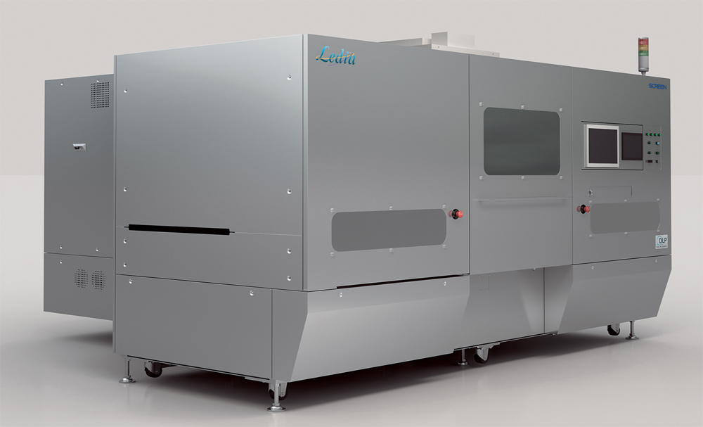
ACB is Europe's leading manufacturer of quick-turn and high-reliability prototype and small series PCBs. Typically an early adopter of new and enabling technologies, the company recently took delivery of a top-of-the-range LED-based Direct Imaging (DI) system from Ucamco. Manufactured by Dainippon Screen, Ledia 5 is the PCB industry's fastest DI system, and the only one capable of processing standard soldermask: unique capabilities that, together with ACB's trust in its suppliers, were key to the company's latest investment decision. Working alongside ACB's existing Laser DI system, Ledia 5 handles all ACB's soldermask processing and provides added capacity for dry film exposure. With it, ACB is more flexible and has improved its product quality, yields and capabilities while offering shorter leadtimes for its quick-turn business.
ACB's CTO Wim Perdu explains
At ACB, we specialise in manufacturing high-technology quick-turn prototype and small series PCBs for clients in the defence, avionics and other demanding sectors. Here, supplier and product reliability is key, speed is of the essence, and board failure is not an option. This means that our client relationships are based on absolute trust in our ability to design and make boards that meet the highest technical specifications and deliver outstanding long term performance in the field.
Whether we are making multi-layers in rigid, flex rigid or flexible constructions, one of our principal strengths is the expertise that we can bring to the early stages of our clients' product development processes, significantly reducing time to manufacture. We do this by ensuring the best possible PCB design, materials and technologies for efficient manufacture and long-term reliability. And we can back up our products with proof of just how well they will perform after 10 or even 20 years of use in the field, thanks to careful but pioneering investments in leading-edge test and evaluation technologies.
Indeed, we have always been quick to recognise the advantages of new technologies and materials. For example, in 2002, we were among the world's first PCB makers to invest in Laser Direct Imaging (LDI), a major step that was instrumental in improving registration and throughput in dry film imaging. Since then, we have always wanted to add extra Direct Imaging (DI) capacity, but only on the condition that it also be capable of exposing standard soldermasks. This is because conventional methods for soldermask exposure are reaching their limits: film movement and bad alignment are limiting high density solder mask design rules and can lead to very expensive scrap.
We have known for some time that the right DI technology would eliminate all of these issues. But soldermasks present some very particular challenges to any exposure process. They are far less photosensitive than dry film resists and coating thickness is variable so it is very difficult to obtain solder mask edges which are perfectly perpendicular to the board, with no undercut or tapering. Thus it is imperative that the soldermask is exposed faultlessly, using the wavelengths to which it is most sensitive. For example, our Taiyo product, like most standard soldermasks, reacts best to a range of different wavelengths. Exposed to all of these, it will polymerise fast and in a reliable, robust way. The single wavelength light sources typical of LDI technology (our existing LDI machine works at 355 nm) are not capable of exposing standard soldermasks. Using them, polymerisation is patchy and slow.
Although special soldermask materials exist that are geared for LDI technologies, these are expensive, and are not a viable option for us anyway. Like all the materials that remain on our boards, our soldermask has undergone lengthy and expensive evaluation and approval procedures by all of our clients, so we intend to continue its use.
So when we heard about the Ledia DI machine from Ucamco General Manager Karel Tavernier, of course we wanted to know more. Dainippon Screen, Ledia's manufacturer, has been developing DI technologies since 2000, and there are now over 70 Ledia machines installed worldwide so it's a proven production tool even though it's light years ahead of other DI technologies. And Ucamco, a long-time supplier of ours, has installed 2 other Ledia systems in Europe over the past 18 months. We have known Ucamco for nearly 20 years – we were one of the first users of the Ucam software, use other Ucamco equipment, and have always worked with the company as a beta site for new solutions. We know that we can trust Ucamco to provide excellent technology and first class support.
Together with the Ucamco team, we carried out in-depth benchmarking evaluations of the Ledia machine, the results of which so impressed us that we opted to install the top-of-the-range machine with 6 exposure heads and 3 cameras for real-time alignment. Each head uses 2 LED light sources, each of which emits its own broad spectrum of wavelengths, so we can tune it to the specific light sensitivity range of the material we are exposing: the better the fit, the less energy is needed to polymerise the material so the faster the process. Using it, we can expose standard soldermask quickly and efficiently, in a robust, reliable process, which makes the Ledia 5 a fantastic drop-in technology for us. It's also a unique proposition for the PCB industry in general: Not only is Ledia 5 the fastest DI machine available today: it is the only one that is capable of processing standard soldermask.
It's excellent for other resists too – it can be tuned precisely to diverse materials with varying characteristics, giving us throughputs that are faster than those possible with our LDI machine. Now, with both machines working side by side, the Ledia machine handles all of our soldermask processing, as well as providing a faster option for outerlayer and innerlayer resist exposure. So we have added manufacturing capacity, more flexibility, better processes and capabilities, and faster turnarounds for our quick-turn business. And our soldermask registration is infinitely better, bringing great improvements in quality and yields.
We've been waiting for Ledia for quite some time. It's a real technology and business enabler for us today, but just as important for us and our clients, as components and their pads become even smaller, we at ACB, with our eyes on the future, feet on the ground, are ready for that too.
Wim Perdu - Chief Technology Officer - ACB NV, Dendermonde, Belgium
Ucamco (formerly Barco ETS) is a market leader in PCB CAM software, photoplotting and direct imaging systems, with a global network of sales and support centers. Headquartered in Ghent, Belgium, Ucamco has over 25 years of ongoing experience in developing and supporting leading-edge photoplotters and front-end tooling solutions for the global PCB industry. Key to this success is the company's uncompromising pursuit of engineering excellence in all its products.
With 200 employees in production facilities in Dendermonde (BE) and Malville (FR), ACB is Europe's fastest supplier of high-end prototype and small series PCBs. Technologies include multi-layers in rigid, flex rigid and flexible constructions for high-reliability sectors such as avionics, space & defence, telecommunications and medical industries. As an engineering partner and strategic supplier, ACB offers manufacturing support through its “early involvement” DfM teams, flexible logistics, and in-house reliability testing and research, as well as through qualified account teams and targeted high-level investment programmes.