PCB Design for Test
Company Information:

Name: |
PCB Design for Test |
Category: |
|
Offered by: |
|
PCB Design for Test Description:
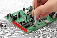
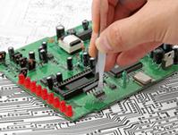
Design-For-Test or DFT takes into account several major and minor considerations at the design layout stage. In this limited webpage space, the key ones are described. However, the overall DFT success for 90 percent plus test coverage relies heavily on implementing all these critical design considerations.
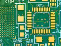
Initially, the PCB design engineer should lay out all test points on one side of the board. Another consideration is maintaining a minimum test point distance from one test point to another. There should be a minimum distance of 100 ml., accounting for about 2.54 millimetres so that probes can perform their job properly.
Test point distribution is important, as well. A high density of test points or clusters should be avoided. Test points should be uniformly distributed throughout the board, making it easier to test with multiple probes and not having to rely on a specific area for all the probes to concentrate on. Moreover, there should be a free zone or a safe zone designated as a keep-out area.
While doing the layout and when feasible, it is a good idea to consider using standard commercial electronic modules, which are available for testing. However, if there are redundant modules, are they being laid out so that they can be tested independently? Put another way, if there's a fault in one module and not in the second, third and fourth, each module should be available for independent testing. Accessibility to each address and data and the bus line is important.
For More information, please visit https://www.technotronix.us/design-for-test.html
PCB Design for Test was added in Aug 2012
PCB Design for Test has been viewed 474 times
9 More Products from Technotronix :