SMT Equipment

RF/Microwave PCB Fabrication: Single Layer - Double Layer - Multi-Layer - Plated Through Holes

Company Information:

ADVANCED CIRCUITRY INTERNATIONAL is a world class supplier of RF/Microwave & Antenna PCB’s with four state-of-the-art facilities on three continents to serve its customers. ACI has the largest RF material stock in North America!

Duluth, Georgia, USA

Consultant / Service Provider, Manufacturer

  • Phone 770-622-2200

See Supplier Website »

Company Postings:

(7) products in the catalog

(2) news releases

RF/Microwave PCB Fabrication: Single Layer - Double Layer - Multi-Layer - Plated Through Holes

RF/Microwave PCB Fabrication: Single Layer - Double Layer - Multi-Layer - Plated Through Holes

Name:

RF/Microwave PCB Fabrication: Single Layer - Double Layer - Multi-Layer - Plated Through Holes

Category:

Fabrication Services

Offered by:

Advanced Circuitry International


RF/Microwave PCB Fabrication: Single Layer - Double Layer - Multi-Layer - Plated Through Holes Description:

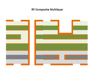
RF & Microwave PCB's

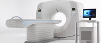
ACI is a leader in providing complex RF/Microwave PCB’s covering a wide spectrum of product types including Defense/Aerospace, Medical Device, Imaging, and Telecommunications Equipment. ACI supports a wide range of frequency bands and has a vast amount of experience utilizing low loss laminates. From multilevel cavity fabrication for vertical and horizontal RF connector launch sites to exotic material composite structures we’re confident delivering reliable and cost efficient products.

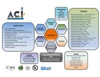
We offer the following expertise and depth of experience:

  • Vast Teflon processing experience
  • Exposed internal cavity RF launch sites
  • OhmegaPly™ & Ticer™ buried resistor technology
  • Precision stub length removal
  • Blind & buried via structures
  • Filled vias and via-in-pad structures
  • Composite multilayers using exotic materials
  • Sequential lamination
  • Castellated vias
  • Precise conductor etching
  • Prototypes to large scale production

Our Capabilities Include: 
Tight Etch Tolerances on Critical RF Features

  • +/- .0005" tolerance on etched features for un-plated 0.5oz copper
  • +/- .001" tolerance on etched features for un-plated 1oz copper
  • Front to back registration of etched cores to +/-.002"
  • Mixed Dielectric constructions
  • Buried & Blind Via constructions
  • Ormet interconnects
  • Multilevel cavity constructions
  • Sequential lamination
  • Plated edges

Back Drill for Precision Stub Removal

  • Mechanical back-drilling (Minimal stub)

Hole Fill

  • Conductive & nonconductive
  • Planarization

Thermal Solutions

  • Metal Back
  • Thermally conductive laminates
  • Screened Heatsink solutions

Embedded Capabilities

  • Planar Resistors
  • Ohmega™
  • Ticer™

Surface Finishes

  • ENIG – electroless nickel, immersion gold
  • ENEPIG - electroless nickel, electroless palladium, immersion gold
  • Hard and soft gold
  • Immersion silver
  • Immersion Tin

Assembly 

  • RF Connectors
  • RF Cabling
  • Antenna Sub-Assemblies
  • Board-to-Board
  • Hand and Robotic Assembly

RF/Microwave PCB Fabrication: Single Layer - Double Layer - Multi-Layer - Plated Through Holes was added in Feb 2017

RF/Microwave PCB Fabrication: Single Layer - Double Layer - Multi-Layer - Plated Through Holes has been viewed 377 times

6 More Products from Advanced Circuitry International :

Reflow Oven

best reflow oven