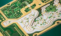
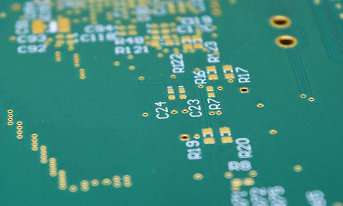
PCB Fabrication
Company Information:
Name: |
PCB Fabrication |
Category: |
|
Offered by: |
|
PCB Fabrication Description:
The layer count of PCB (Printed Circuit Board) determines its manufacturing technology difficulty and PCB manufacturing cost. PCB boards can be briefly classified into two categories: single-layer (single-sided) PCB and double-layer (double-sided) PCB. When it comes to high-end electronic products, a couple of signal layers can be added to the inside of PCB apart from surface routing due to some limitations in terms of board real estate and board design. During the manufacturing procedure, after routing for each layer has been finished with positioning and lamination completed, multiple layers of signals will be pressed into a single board that is called multilayer PCB. Therefore, a multilayer PCB refers to any piece of circuit board containing more than two layers of signals. Multilayer PCBs can be multilayer rigid PCB, multilayer flex PCB and flex-rigid multilayer PCB.Multilayer PCB Fabrication.
Necessity of Multilayer PCB
Due to the increasing use of IC (Integrated Circuit) package, interconnection lines become so dense that multi-substrate boards become necessary. In addition, some design problems, like noise, stray capacitance, crosstalk etc., are so protruding that should be solved through multilayer resolution. As a result, PCB design has to make sure that signal lines should be minimized and parallel circuits should be avoided, which is apparently difficult to be obtained in either single-sided or double-sided design. Therefore, multilayer PCBs come into being for the acquisition of perfect performance of circuits.
The original aim of multilayer PCB is to provide more freedom in terms of routing for circuits that are complex and/or sensitive to noise. There are at least three layers in a multilayer PCB and two layers are external with the left layer(s) synthesized inside insulating plate. The electrical connection in a multilayer PCB derives from plated through hole on the cross section of circuit board.
Advantages of Multilayer PCB
• Smaller size
• Lower weight
• Higher speed of signal transmission
• Constantly low impedance
• Better shielding effect
• Higher assembly density
| Standard Features | Standard | Advanced |
| Maximum Layer Count | 46L | 100L |
| Maximum Panel Size | 21×24″ | 24×42″ |
| Outer Layer Trace/Spacing | 50µm/50µm | 40µm/40µm |
| (1/3oz starting foil + platig) | [0.0035″/0.0035″] | [0.0025″/0.003″] |
| Inner Layer Trace/Spacing | 45µm/45µm | 35µm/35µm |
| (Hoz inner layer cu) | [0.003″/0.003″] | [0.002″/0.002″] |
| Maximum PCB Thickness | 3.2mm | 6.5mm |
| Minimum PCB Thickness | 0.20mm (8mil) | 0.10mm (4mil) |
| Minimum Mechancial Drill Size | 0.20mm (8mil) | 0.10mm (4mil) |
| Minimum Laser Drill Size | 0.10mm (4mil) | 0.08mm (3mil) |
| Maximum PCB Aspect Ratio | 10:01 | 25:01:00 |
| Maximum Copper Weight | 5 oz [178µm] | 30 oz [1050µm] |
| Minimum Copper Weight | 1/3 oz [12µm] | 1/4 oz [9µm] |
| Minimum Core Thickness | 40µm | 16µm |
| Minimum Dielectric Thickness | 30µm | 12µm |
| Minimum Pad Size Over Drill | 0.46mm | 0.4mm |
| Solder Mask Registration | ± 50µm | ± 25µm |
| Minimum Solder Mask Dam | 76µm | 64µm |
| Copper Feature to Edge, V‐cut (30°) | 0.40mm | 0.36mm |
| Copper Feature to PCB Edge, Routed | 0.25mm | 0.20mm |
| Tolerance on Overall | ± 100µm | ±50µm |
| Technologies | Standard | Advanced |
| Rigid‐Flex & Flexible Circuits | Y | Y |
| Buried and Blind Vias | Y | Y |
| Sequential Lamination | Y | Y |
| Impedance Control | ± 10% | ± 5% |
| Hybrids & Mixed Dielectrics | Y | Y |
| Aluminum PCB’s | Y | Y |
| Non‐Conductive Via Fill (VIP) | Y | Y |
| Conductive Via Fill | Y | Y |
| Cavity Boards | Y | Y |
| Backdrilling | Y | Y |
| Controlled Depth Drill and Rout | Y | Y |
| Edge Plating | Y | Y |
| Buried Capacitance | Y | Y |
| Etch Back | Y | Y |
| In‐board Beveling | Y | Y |
| 2‐D Bar Code Printing | Y | Y |
Multilayer PCBs can be served in so many industries including consumer electronics, medical care, aerospace, telecommunications, military, automotive, wearables, IoT etc. based on its benefits. Alcanta PCB has been striving to provide high-quality multilayer PCBs for customers with full concerns in terms of design, cost and lead time. Contact us and follow rainbows with Alcanta PCB!
PCB Fabrication was added in Jul 2020
PCB Fabrication has been viewed 121 times