Mar 11, 2013
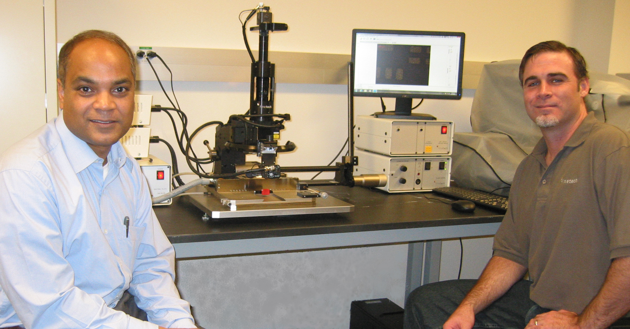
A FINEPLACER® Pico bonder has been installed at the MEMS Nanoscale and Devices Group at Pennsylvania State University. As part of the company’s 20th anniversary last year, Finetech held a donation drawing for a $100,000 high-accuracy bonding system that was open to universities and colleges. This was Finetech’s way of giving back to the university R&D segment of its business. Penn State was the randomly selected winner out of nearly 400 entries.
“We have been using the Pico bonder for a couple of months now and are pleased to have added high-accuracy bonding capabilities to our facility,” states Srinivas Tadigadapa, Pennsylvania State University, Professor, College of Engineering ― MEMS Nanoscale and Devices Group. “We are able to use it for our MEMS device packaging, microfluidic devices and laser diode devices research. The students particularly like the user interface of the machine and appreciate the high accuracy placement of aligned dies.”
With a wide installed base of systems at many prestigious institutions, FINEPLACER® die bonders provide an ideal solution for advanced technology environments utilizing diverse applications. The FINEPLACER® Pico bonder is an ‘all-in-one’ platform for precise packaging and assembly applications, such as flip chip, optoelectronics, 3-D, wafer-level integration, micro-optics assembly, sensor packaging and precise die bonding.
For more information about Finetech, visit http://www.finetechusa.com.
For more information about the MEMS Nanoscale and Devices Group, visit http://mnd.ee.psu.edu/index.asp.
Finetech is a leading manufacturer of equipment for manual and fully automatic component rework and high-precision bonding and die attach. The company services customers in a broad range of industries including aerospace, medical technology, consumer electronics, semiconductor, optoelectronics, military, universities and research. Finetech offers a flexible approach to customer support and welcomes the opportunity to create customized, effective solutions. Corporate headquarters and main production are in Berlin, Germany. Sales and Technical support centers are located in Tempe, Arizona; Manchester, New Hampshire; Shanghai, China and Kuala Lumpur, Malaysia.
Pennsylvania State University – MEMS Nanoscale and Devices Group
The Pennsylvania State Electrical Engineering Department, established in 1893, is among the largest, oldest, and most innovative in the nation. The main focus of the department’s Micro & Nanoscale Devices Group is to design, model, and fabricate devices using MEMS fabrication technologies for transducer applications and investigation of interfacial science at the nanoscale. Research areas include: materials and devices for electronic, photonic, bioelectronic and MEMS applications, amorphous and crystalline silicon, III-V compounds, organic thin films, ferroelectric and piezo-electric; development of novel device structures and manufacturing methods, device and circuit simulation and modeling, device and material characterization