Oct 12, 2011
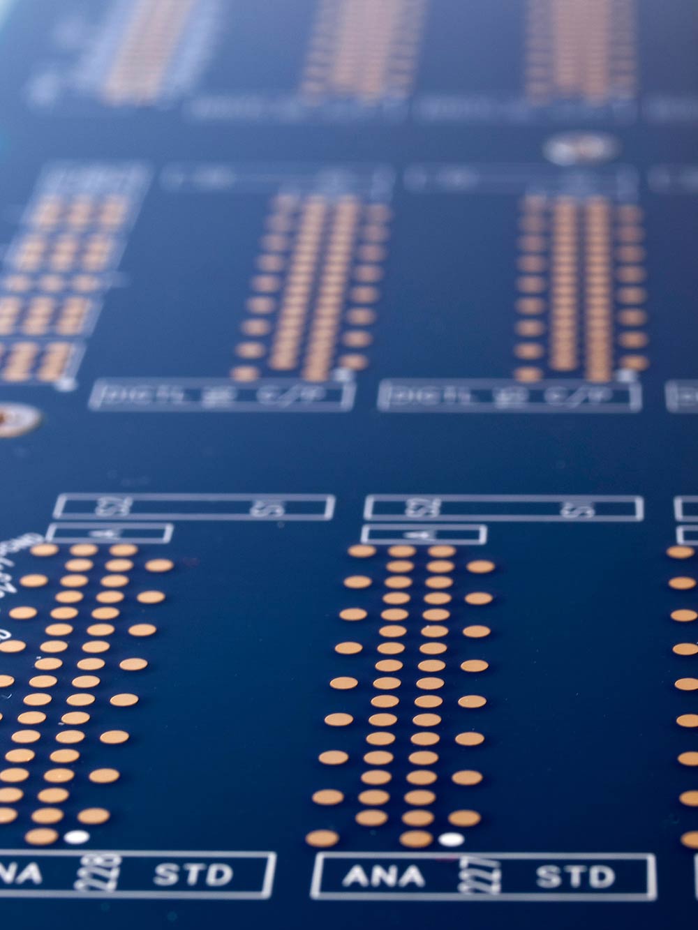
Multitest’s board fab leverages the benefits of pulse plating
Multitest, a designer and manufacturer of final test handlers, contactors and load boards used by integrated device manufacturers (IDMs) and final test subcontractors worldwide, announces that the Santa Clara board fab has refined its pulse plating process to integrate it into Multitest’s fabrication process to further enhance the high aspect ratio capability. The integration is a result of the Santa Clara board fab anticipating the market trend for chip scale packages, particularly for fine-pitch array packages such as BGAs or LGAs.
Leveraging the advantages of its continually refined manufacturing process, Multitest now is able to build 0.3 mm through-hole constructions and boards with even higher layer count for high pin count, 0.4 mm fine-pitch array applications.
Multitest is known for leading drilling and registration competence. The company continues to invest in high aspect ratio via capabilities to continuously enhance the fine-pitch product offering.
Multitest (headquartered in Rosenheim, Germany) is one of the world’s leading manufacturers of test equipment for semiconductors. Multitest markets test handlers, contactors, and ATE printed circuit boards. Globally, more than 700 employees serve the company’s customers in offices and branches in North America, Singapore, Malaysia, the Philippines, Taiwan, China and Thailand.